
 I'm LongbridgeAI. Here is the key information I extracted
- China is expected to add 16GW of perovskite capacity in 2026, and major companies have begun mass production, indicating a shift towards competitive technology against traditional silicon-based solar cells. …
The years 2025-2026 mark a historic turning point for the perovskite photovoltaic industry as it transitions from "technology validation" to "mass production." Driven by a confluence of breakthroughs in efficiency records, the gradual commissioning of GW-level production lines, and the opening up of disruptive application scenarios (space photovoltaics, BIPV, flexible electronics), market attention is rising exponentially. Perovskite technology not only represents an "efficiency improvement and cost reduction" enhancement to traditional crystalline silicon routes but also systematically reshapes the forms of photovoltaic products, application boundaries, and the industrial value chain.
A comprehensive understanding of the perovskite industry.
I. What Happened? From Technology to Mass Production
2025 is referred to as the "Year of GW-level Production Line Commissioning" for perovskite, marking the official transition of technology from the laboratory to mass production. The year 2026 will witness a critical moment of concentrated capacity release and the realization of commercial orders. The core logic of perovskite batteries is to become a strong competitor in the ultimate photovoltaic technology route by leveraging extreme theoretical efficiency (33% for single junction, over 45% for tandem) and a disruptive cost structure (single factory integration, reducing process time from 3 days to 45 minutes).
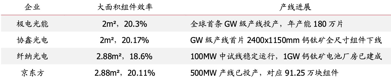
In 2026, China's new perovskite production capacity is expected to reach 16GW, with leading companies such as GCL-Poly and Jidong Energy entering the GW-level component mass production verification stage.
In the past year, the industry has completed the most challenging leap from "0 to 1."
In February 2025, Jidong Energy achieved the industry's first GW-level perovskite component mass production; in October, GCL-Poly's GW-level production line rolled off its first full-size component measuring 2.4m×1.15m. This means that the size of perovskite components has caught up with crystalline silicon, laying the foundation for large-scale ground station applications. BOE's 2.88m² large-size component achieved a breakthrough of 20.11% in overall area efficiency in 2025. Previously, the efficiency decay of large areas had been a "ghost" hindering the industrialization of perovskite, and crossing the 20% threshold means it has secured a ticket to compete on the same stage as crystalline silicon.
In addition to pioneers like GCL-Poly, Xina, and Jidong, the deep involvement of cross-industry giants such as BOE, CATL, and BYD has brought substantial capital and semiconductor-level manufacturing process thinking to the industry.
The reason for the skyrocketing market attention on perovskite is that people realize its core logic lies not in patching crystalline silicon but in revolutionizing the entire production method of the photovoltaic industry chain.
① Extreme Efficiency Ceiling
The theoretical maximum efficiency of crystalline silicon batteries is about 29.4%, and the industrialization is currently approaching the bottleneck of 26%. In contrast, the theoretical limit for single-junction perovskite reaches 33%, and all-perovskite tandem can even exceed 45%. In the "efficiency is king" industry of photovoltaics, every 1% improvement translates to a significant reduction in LCOE (levelized cost of electricity) ② Disruptive Cost Structure (“Single Factory Equals Full Chain”)
Traditional crystalline silicon model: Silicon materials, wafers, cells, and modules are produced in different factories, requiring more than 3 days for the entire process, involving a large number of high-temperature processes (silicon refining above 1400℃).
Perovskite model: Within a single factory, the process is completed in one go from glass substrate entry, coating, vapor deposition, to packaging, with the entire temperature not exceeding 150℃. It takes about 45 minutes from raw materials to module delivery.
Capital expenditure: The investment for perovskite single GW capacity is expected to drop to about half that of crystalline silicon. Against the backdrop of fluctuating energy costs in 2026, the low energy consumption characteristics of perovskite have strong premium potential.
③ Significant Expansion of Application Scenarios
Perovskite has characteristics such as lightweight, flexibility, translucency, and good performance in low light. This allows photovoltaics to no longer be limited to rooftops and ground installations but to perfectly integrate into BIPV (Building Integrated Photovoltaics), vehicle-mounted photovoltaics, flexible electronics, and even space photovoltaics.
II. Why is it Important? Strong Industry Demand
Space photovoltaics have fully opened market attention, and perovskite technology will systematically reshape the forms of photovoltaic products, application boundaries, and industrial value chains. Downstream demand anchors are emerging, especially the grand narrative of "space photovoltaics" will further drive industry technology and capital expenditure.
SpaceX founder Elon Musk proposed a plan to build 100GW of space photovoltaics annually after 2029 to support its "orbital data center" (one million V3 satellites). Perovskite batteries, with their extremely high power-to-weight ratio (10-30W/g, 30-80 times that of gallium arsenide), extremely low estimated costs (1/10 of gallium arsenide), and excellent flexibility and radiation resistance, are widely regarded as the only feasible technological path to achieve this grand vision. This long-term demand anchor from the world's most influential technology leader brings unprecedented imaginative space and certainty expectations for perovskite. 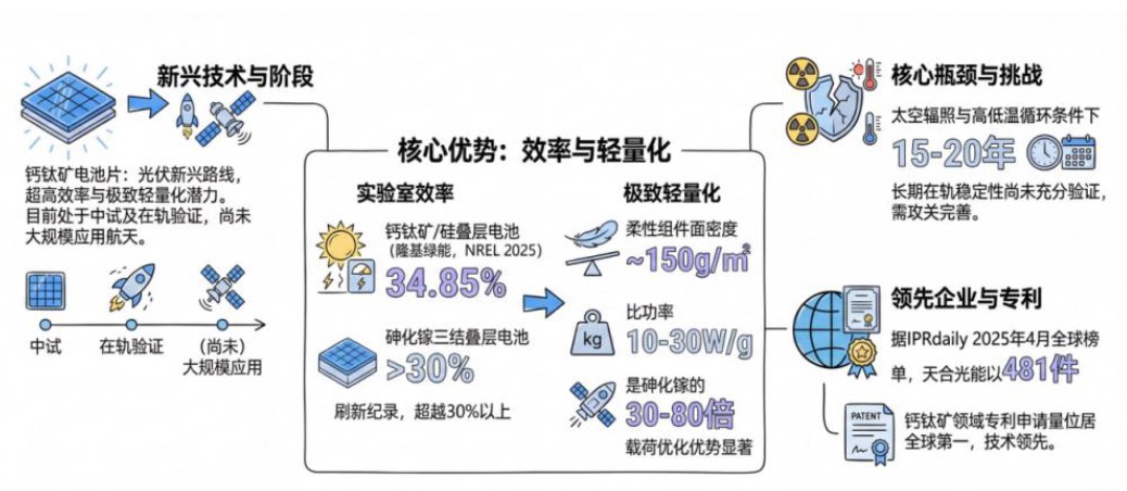
To clarify the understanding, we must first understand why perovskite is the "key variable" in reshaping the landscape?
In addition to the efficiency and cost advantages we discussed in the first part, more importantly, the breakthrough of perovskite from "standard products" to "customized products" opens up the value ceiling of photovoltaics. Traditional crystalline silicon modules are highly standardized industrial products, difficult to escape the fate of being a commodity. However, the flexible, transparent, and colorful characteristics of perovskite allow it to deeply integrate with buildings, automobiles, and consumer goods, transforming from a mere "power generation functional component" into a "power generation functional material" with aesthetic value and design integration value, thus breaking free from low-price competition and obtaining brand and design premiums. 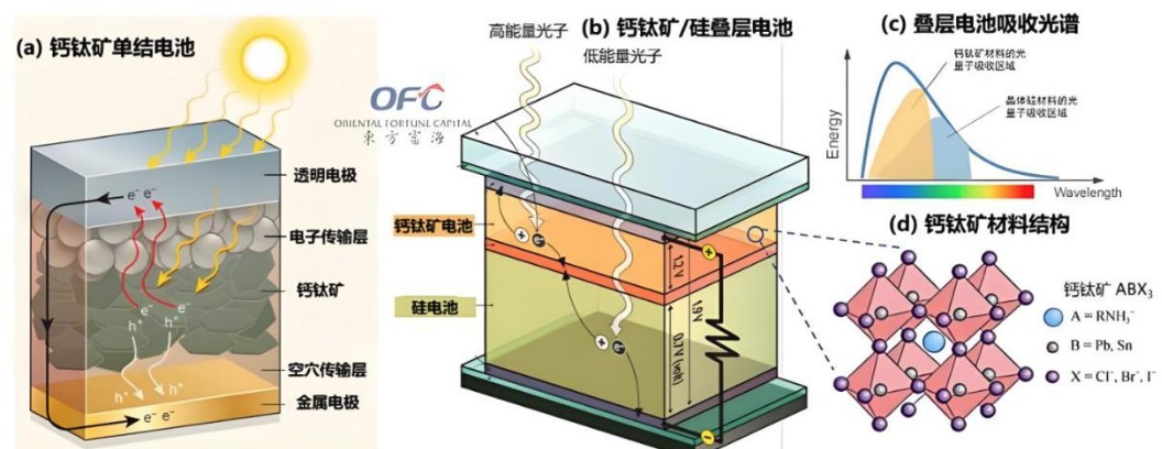 Perovskite is the "energy key" to unlocking large-scale space economic activities (giant constellations, orbital data centers, deep space exploration). Without the magnitude of weight and cost improvements brought by perovskite, Musk's space computing blueprint is merely a castle in the air. This elevates its strategic significance to the height of national space competitiveness.
For China's manufacturing industry, this represents another strategic opportunity to lead global industrial transformation. China has formed a synergistic advantage in the perovskite field characterized by "leading in academia - radical in industry - active in capital." From efficiency records, GW-level production line progress to supporting equipment and material supply chains, China is in the global first tier. Perovskite marks the first time China has synchronized with or even outpaced the world in the industrialization race of a disruptive photovoltaic technology after experiencing the "introduction - digestion - leadership" of crystalline silicon technology. Successfully seizing this opportunity means that China can not only consolidate its absolute leading position in the global photovoltaic manufacturing industry but also dominate the standard-setting, intellectual property, and high-end application markets of the next generation of energy technologies.
III. What to focus on next? Core link value
In the early stages of perovskite development, we tend to look for certainty opportunities in the "shovel sellers" and "high-barrier auxiliary materials" of the industrial chain. 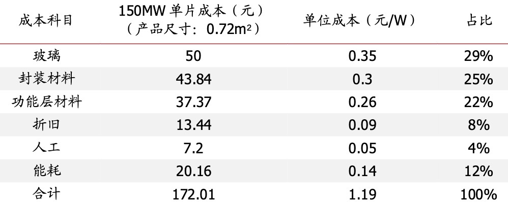
① Core equipment segment: The most valuable high ground
The manufacturing of perovskite involves a large number of precision equipment, with extremely high barriers:
Coating equipment (Slot-die): Controls the uniformity of nanoscale films. Focus on domestic alternatives with semiconductor-level coating technology accumulation.
Deposition equipment (PVD/RPD/CVD): Key deposition equipment for the perovskite layer and transport layer. Particularly, RPD (Reactive Plasma Deposition) has unique advantages in protecting the perovskite surface.
Laser equipment: The four laser scribing (P1-P4) determines the effective power generation area and resistance loss of the module, with extremely high precision requirements. 
② Key materials segment: A new cycle of structural expansion
Rubidium/Cesium salt additives: Rubidium (Rb) and Cesium (Cs) can significantly enhance the stability and photoelectric performance of perovskite. With the capacity release in 2026, the rubidium salt market is entering a new cycle of structural expansion. This is an undervalued hidden asset in the market.
TCO conductive glass: Perovskite has higher requirements for the transmittance and conductivity of glass than crystalline silicon, and FTO glass, among others, will see a demand explosion.
Hole transport materials: Such as Spiro-OMeTAD or new self-assembled monolayers (SAMs), these high-value chemicals are key to improving efficiency.
At the event node in 2026, we recommend focusing on the following industrial rhythms: ① GCL-Poly Solar: Industry benchmark, pay attention to its GW-level production line's ramp-up yield and BIPV order signing.
② Jidian Energy: One of the fastest companies to realize GW-level production capacity, observe its empirical data in large-scale ground power stations.
③ BOE Technology Group: Focus on how it utilizes display panel technology to cross over and replicate in controlling the uniformity of perovskite on a large scale.
④ Rubidium/Cesium mineral resource providers: Those with globally high-quality cesium mineral resources are scarce targets and suppliers at the top of the industry chain. 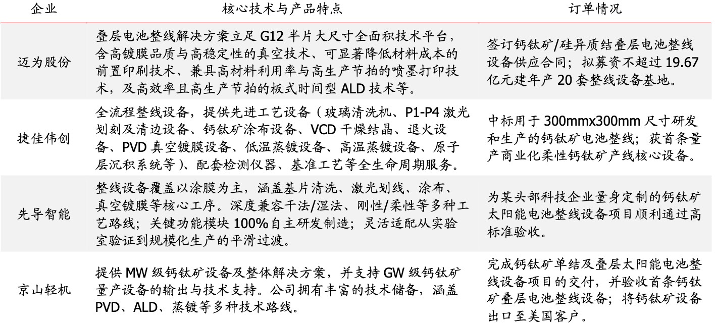
Of course, the perovskite industry will face key challenges in 2026—although production capacity has increased, it still needs to address the "three soul questions":
① Longevity stability: Although laboratories can pass IEC aging tests, can components from GW-level production lines maintain 20-25 years in the field? This is crucial for application.
② Consistency of large-area efficiency: From 30cm² to 2.88m², how to ensure the uniformity of every inch of the film?
③ Lead leakage and environmental protection: Although the lead content is extremely low, building a recycling system for the entire lifecycle is a necessary condition for entering markets like the EU.
It is expected that by 2030, global perovskite new production capacity will exceed 180GW. By then, perovskite will not only supplement crystalline silicon but will also dominate in the fields of space photovoltaics, BIPV, and high-performance power stations.
Risk Warning and Disclaimer
The market has risks, and investment should be cautious. This article does not constitute personal investment advice and does not consider individual users' specific investment goals, financial conditions, or needs. Users should consider whether any opinions, views, or conclusions in this article align with their specific circumstances. Investment based on this is at one's own risk