
Terafab lands: $16.8 billion Phase I investment, how to rewrite the boundaries of Tesla's chip manufacturing?
 I'm LongbridgeAI, I can summarize articles.
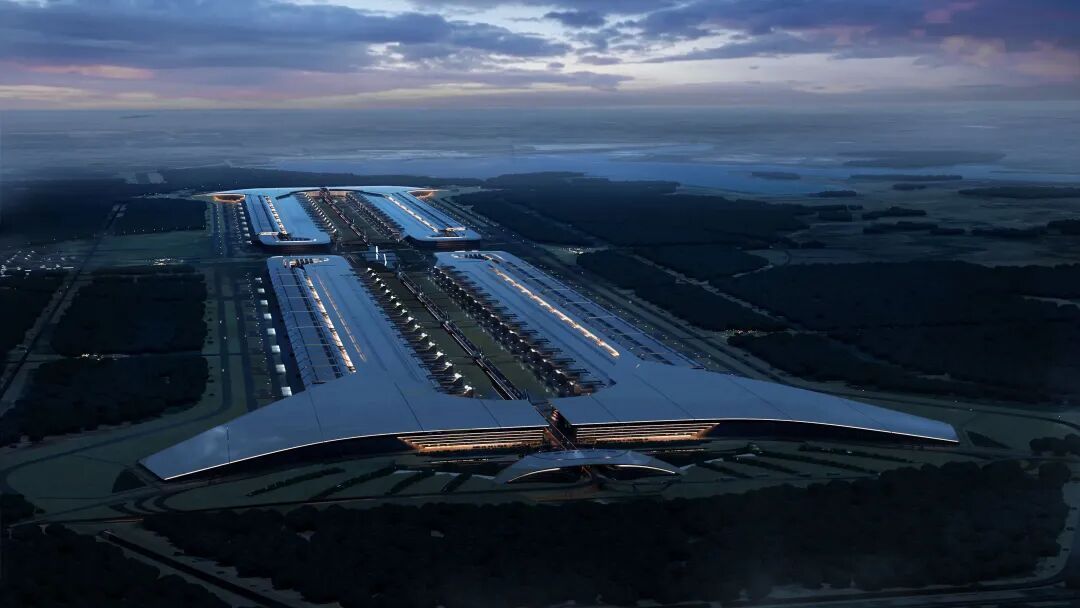
Official rendering of the Terafab Grimes County project | Source: SpaceX
I. Project Enters Engineering Phase: $16.8 Billion Corresponds Only to Phase I
On August 6, the Governor's Office of Texas confirmed that SpaceX will build the vertically integrated semiconductor manufacturing base Terafab in Grimes County. The capital investment for Phase I exceeds $16.8 billion, with plans to create 3,000 new jobs and receive a $30 million grant from the Texas Enterprise Fund. The project location, construction entity, and initial investment have been confirmed by government announcements; subsequent research can shift focus to construction pace and equipment orders.[1]
The JETI application file from the Texas Comptroller's Office presents a larger long-term framework. Terafab is defined as a vertically integrated semiconductor manufacturing and advanced computing facility, covering IC design, photomasks, wafer fabrication, advanced packaging, and system-level integration, proposing processes below the 2nm level. The project will be built in up to four phases, with capital investment ranges between $55 billion and $119 billion in the documents; subsequent expansion still depends on demand realization, process maturity, and capacity ramp-up.[2]
It is necessary to model the Austin Research Fab separately from the large-scale Terafab in Grimes County. The former, located at Giga Texas, undertakes prototype manufacturing, process verification, and technology transfer; the latter corresponds to subsequent mass production. Merging both into Tesla's capital expenditures would simultaneously overestimate TSLA's direct cash outlays and misjudge the timing of equipment order recognition.
II. Process Boundaries Are Clear: Advanced Logic, Memory, and Packaging Enter the Same System
Tesla's public recruitment has provided relatively specific process boundaries. The Terafab Process Integration role requires experience in 2nm-class processes, Gate-All-Around (GAA), High-NA EUV, backside power delivery, and heterogeneous integration such as CoWoS/SoIC; the Lithography role covers EUV, ArFi, exposure tool verification, and internal photomask lines; the Memory role involves the design and process integration of DRAM, LPDDR, and HBM.[3][4]
The difficulty of this manufacturing system is higher than that of a single advanced logic wafer fab. The logic side involves GAA, advanced interconnects, EUV, and backside power delivery; the memory side involves high aspect ratio etching, capacitor structures, data retention, and memory bit yield; advanced packaging further couples logic, memory, and interconnect yields. Equipment can be purchased, but stable process windows, defect density, and mass production yields can only be accumulated through long-term engineering data.
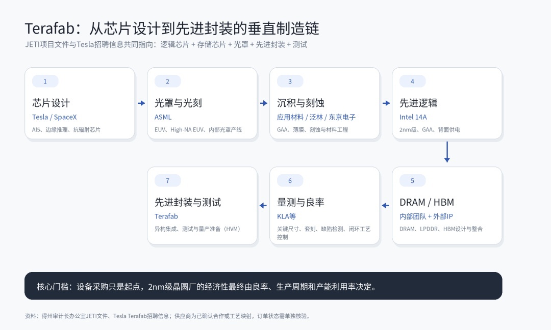
Terafab Vertical Integration Manufacturing Chain | Self-made; Data: Texas Comptroller's Office JETI Document, Tesla Terafab Recruitment Information.
For Tesla, the core value of the manufacturing end lies in locking in internal demand. AI5 and subsequent edge inference chips serve vehicles, Robotaxi, and Optimus; SpaceX brings radiation-hardened chips and orbital computing needs; xAI corresponds to training and inference infrastructure. When terminal demand is sufficiently large, internal demand can support equipment utilization rates and shorten the design-manufacturing iteration cycle; if demand realization lags behind capacity construction, high depreciation will quickly drive up unit chip costs.
III. Intel 14A Provides Process Anchor, Mass Production Engineering Remains Core Shortcoming
In April, Intel confirmed joining the Terafab project; subsequently, Musk stated plans to adopt Intel's next-generation 14A process. For Intel, the strategic weight of this cooperation is higher than ordinary foundry orders: 14A requires large external customers to verify process maturity and the commercial model of wafer foundries, while Terafab needs mature advanced process experience to shorten the cycle from equipment installation to stable mass production at newly built wafer fabs.[5]
Intel officially defines 14A as a combination of RibbonFET 2 Gate-All-Around and PowerDirect backside power delivery, targeting a 15%–20% performance increase at the same power consumption, a 25%–35% power reduction at the same performance, and a density increase of up to approximately 30% relative to 18A. ASML EXE:5200B is then aimed at High-NA EUV mass production for logic and advanced DRAM below 2nm.[6][7]
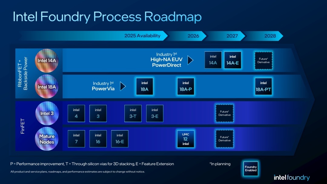
Intel Foundry Official Process Roadmap | 14A involves High-NA EUV and PowerDirect; Source: Intel Foundry.
The gap between Terafab and mature wafer foundries is mainly concentrated in process integration and large-scale mass production (HVM). Barriers to advanced wafer fabs include yield learning curves, equipment matching, overlay and critical dimension control, defect detection, process recipe stability, and continuous manufacturing organization. Tesla's metrology roles have listed platforms such as KLA, ASML, Hitachi, and Bruker in their experience requirements, emphasizing closed-loop process control and yield improvement, indicating that the project is currently still in the stage of building mass production methodology and engineering systems.[8]
IV. Comparing TSMC, Samsung, and Intel Foundry: Terafab Fights for Supply Control
| Model | Core Advantage | Main Constraint | Terafab Research Focus |
|---|---|---|---|
| TSMC | Leading process yield, customer portfolio, equipment utilization, and economies of scale | Customers need to accept wafer foundry capacity allocation and external supply cycles | Whether internal demand can support sufficiently high capacity utilization |
| Samsung Foundry | Relatively complete synergy foundation of logic chips + memory + advanced packaging | Advanced logic yield and customer stickiness still need continuous verification | Its integrated model is the closest industrial reference for Terafab |
| Intel Foundry | 14A, GAA, backside power delivery, and US domestic manufacturing capabilities | The scale of external wafer foundry customers and loss convergence remain core issues | Terafab may become an important external validation scenario for 14A |
| Terafab | Internal demand from Tesla / SpaceX / xAI, shorter design-manufacturing feedback cycle | Yield, manufacturing organization, equipment utilization, and huge capital expenditures | Whether unit computing cost can be lower than the comprehensive cost of external foundry + memory + packaging |
Whether Terafab can succeed ultimately depends on unit computing cost, not nominal capacity. AI5, Robotaxi, Optimus, and SpaceX must provide sufficiently large internal wafer demand to support advanced wafer fabs in maintaining high utilization rates for the long term, and reduce unit manufacturing costs through synergy in chip design, memory interfaces, and advanced packaging. If terminal shipments lag behind capacity deployment rhythms, equipment depreciation and fixed costs will directly drag down the cost curve, and self-built wafer fabs may instead become a pressure source for capital returns.
V. Capital Expenditure Flows to Equipment First: ASML, AMAT, LRCX Have Shorter Realization Paths
Phase I exceeding $16.8 billion does not equal $16.8 billion in wafer fabrication equipment (WFE) orders. Total wafer fab investment also includes land, buildings, cleanrooms, plant services, electricity, water treatment, automated logistics, and supporting infrastructure. It is more suitable at this stage to use scenario analysis to calculate equipment value; one cannot treat a certain equipment proportion as a given procurement structure.
According to public evidence, Intel has officially joined the project; ASML CEO confirmed discussing Terafab with Musk; Bloomberg previously reported that the project team inquired about equipment quotes and lead times from Applied Materials, Lam Research, Tokyo Electron, etc., with Reuters noting it could not independently verify. KLA's benefit logic mainly comes from Tesla's metrology roles explicitly requiring platform experience, but there is currently still a lack of public evidence of formal large orders from Terafab.[9][10]
| Company | Terafab Mapping | Current Evidence | Performance Transmission Judgment |
|---|---|---|---|
| Intel | 14A Process / Manufacturing Capability | Confirmed to join the project | High strategic validation value; wafer foundry revenue elasticity depends on actual wafer volume |
| ASML | EUV / High-NA EUV | Management confirmed communication on the project; high technological irreplaceability | High value per unit of equipment; revenue recognition constrained by installation pace |
| AMAT | Deposition, Materials Engineering | Media reports indicate inclusion in inquiry scope | Increased advanced process steps raise unit capacity equipment investment |
| LRCX | Etching, Deposition, Cleaning | Media reports indicate inclusion in inquiry scope | GAA / Memory high aspect ratio processes increase equipment value |
| KLA | Metrology, Defect Detection, Process Control | Tesla recruitment explicitly requires relevant platform experience | Rigid demand during yield ramp-up phase; public order evidence remains weak |
During the construction period, revenue recognition for wafer fabrication equipment (WFE) manufacturers usually precedes the formation of wafer fab's own chip profits. Terafab at this stage is closer to "equipment order catalyst," and TSLA's short-term EPS still needs to wait for capacity, yield, and terminal demand to jointly verify.
VI. Tesla Capital Expenditure Has Already Led: H1 Free Cash Flow Only About $350 Million
In the first half of 2026, Tesla achieved revenue of $50.62 billion and operating cash flow of $8.63 billion; meanwhile, capital expenditures were $8.28 billion, an increase of about 113% compared to $3.89 billion in the same period of 2025, with free cash flow only about $350 million. R&D expenses were $4.32 billion, a year-on-year increase of 44%, with the revenue share rising from 7% to 9%, incremental mainly coming from AI and other R&D projects.[11]
Tesla's full-year capital expenditure in 2025 was $8.53 billion; by the second quarter of 2026, the company had raised its full-year capital expenditure expectation to over $25 billion, mainly invested in AI computing power and data centers, manufacturing and R&D production lines, and AI-related assets. Capital intensity has clearly broken away from the interval previously driven mainly by automotive capacity expansion.[12]
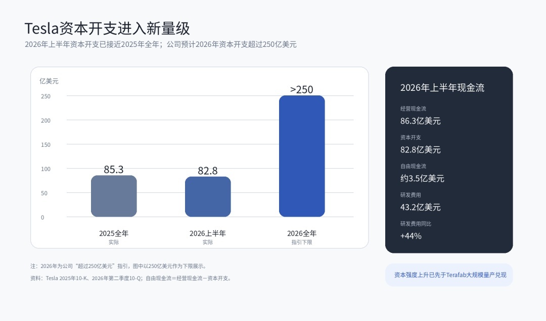
Tesla Capital Expenditure and H1 2026 Cash Flow | Self-made; Data: Tesla 2025 10-K, Q2 2026 10-Q.
This set of data constitutes the realistic constraint on Terafab valuation. The $16.8 billion for Phase I in Grimes County cannot all be counted in TSLA's financial statements, but Tesla's own R&D wafer fab, AI infrastructure, computing clusters, Robotaxi, and Optimus manufacturing are already synchronously consuming cash. If subsequent equity and equipment financing arrangements increase Tesla's direct contribution ratio, free cash flow and depreciation pressure will continue to rise.
VII. Valuation: Long-term Supply Certainty Increases, But Not Enough to Sustainably Support TSLA Valuation Upgrade Alone
As of the US stock market close on August 6, TSLA was quoted at $319.53, with a market cap of approximately $1.13 trillion, and a static P/E ratio of about 296 times. Tesla's 2025 revenue was $94.83 billion, and H1 2026 revenue was $50.62 billion; calculated on a trailing twelve months (TTM) basis, revenue is approximately $103.6 billion, corresponding to a Price-to-Sales (P/S) ratio of about 10.9 times.
This valuation has already factored in long-term options such as Robotaxi, Optimus, AI software, energy business, and manufacturing vertical integration. Terafab improves the controllability of AI chip supply, but short-term financial performance is still dominated by capital expenditures, R&D expenses, and future depreciation. The variables that can truly adjust the profit model are mainly three: the actual wafer demand for AI5 and subsequent chips, the yield after the R&D wafer fab transfers to large-scale manufacturing, and the final project capital proportion borne by Tesla.
If Robotaxi and Optimus enter million-level deployment, while Terafab maintains high capacity utilization, internalizing advanced logic, memory, and packaging has the opportunity to reduce unit inference costs and shorten chip iteration cycles; if terminal demand is lower than capacity planning, the decline in wafer fab asset turnover will directly form a valuation discount.
Viewpoint: High Strategic Value, Limited Short-term Profit Elasticity, Watch Orders in Equipment Chain First
TSLA: Terafab increases long-term AI chip supply certainty, but the current rolling P/S of about 10.9 times and near 300 times static P/E already contain high long-term expectations. Capital expenditures exceed $25 billion in 2026, with H1 free cash flow near break-even; continued valuation expansion requires terminal AI businesses to form verifiable cash returns.
Equipment Chain: The performance mapping paths for ASML, AMAT, and LRCX are shorter; KLA benefits from the rigid demand for yield control, but order evidence still needs tracking. After the project enters formal installation, equipment orders and revenue recognition will lead Terafab's own profits.
Intel: If 14A enters mass production in Terafab, the value is mainly reflected in external customer validation and wafer foundry capacity utilization, rather than a single equipment transaction. This cooperation's significance to Intel's manufacturing strategy is clearly higher than its contribution to TSLA's recent profits.
The five nodes most worth tracking subsequently are, in order: formal equipment purchase orders, Intel 14A technology transfer, first batch of wafers and yield from the Austin R&D wafer fab, installation progress of Phase I in Grimes County, and disclosure of the final capital bearing and asset ownership of Terafab by Tesla/SpaceX. Any substantial change in these items will change earnings forecasts more than the project's nominal investment amount itself.
Sources and Scope
- Texas Governor's Office: Governor Abbott Announces SpaceX Expansion In Grimes County, 2026-08-06
- Texas Comptroller's Office: TERAFAB Advanced Semiconductor Manufacturing Facility JETI Application
- Tesla Recruitment: Sr. Process Integration Engineer, Terafab
- Tesla Recruitment: Sr. Process Engineer, Lithography, Terafab
- Reuters: Intel joins Musk’s Terafab AI chip project, 2026-04-07
- Intel Foundry: Semiconductor Manufacturing Process Technologies
- ASML: TWINSCAN EXE:5200B
- Tesla Recruitment: Sr. Metrology Engineer, Terafab
- ASML: EUV lithography systems
- Reuters / Bloomberg: Terafab supplier outreach, 2026-04-15
- Tesla Q2 2026 Form 10-Q
- Tesla 2025 Form 10-K
This article is only for industry research and information exchange, and does not constitute securities trading advice. Content involving forward-looking investments, supplier shares, and mass production schedules, unless noted as official disclosures by companies or governments, is scenario analysis based on public information; subsequent updates will follow company announcements, regulatory documents, and formal orders.










The copyright of this article belongs to the original author/organization.
The views expressed herein are solely those of the author and do not reflect the stance of the platform. The content is intended for investment reference purposes only and shall not be considered as investment advice. Please contact us if you have any questions or suggestions regarding the content services provided by the platform.