
D
17 hours ago
If NAND is 'born prolific,' how does SanDisk defend an 80% GPM?
 I'm LongbridgeAI, I can summarize articles.
In the prior piece 'AI inference boom: can the 'unlucky' SanDisk really rise from the ashes?', Dolphin Research noted that after shedding its legacy HDD burden, SanDisk fully pivoted to NAND and captured the cyclical upturn. The AI inference boom has been a timely tailwind for the company.
On tech, SanDisk avoids chasing layer counts blindly and instead drives lateral scaling to achieve industry-leading areal density. It pioneered CBA bonding in volume to boost energy efficiency and co-launched HBF (High Bandwidth Flash) tailored for AI inference. These moves keep its NAND capabilities firmly in the first tier.
With the NAND cycle turning, SanDisk’s results are primed to inflect. This report dives into three core topics.
1) What kind of industry was NAND before the AI wave?
2) Why does NAND supply repeatedly get trapped in a 'can’t-cut' cycle?
3) DRAM vs. NAND: same memory roots, very different outcomes.
正文如下:
I. What was NAND before the AI wave?
Break SanDisk’s 2019–2025 flash biz into volume and price and you get a rare pattern for manufacturing. The shape is counterintuitive.
Bit shipments jumped from 38 EB to 101 EB, up 166% over six years. Yet ASP per GB fell from $0.206 to $0.073, down 65%.
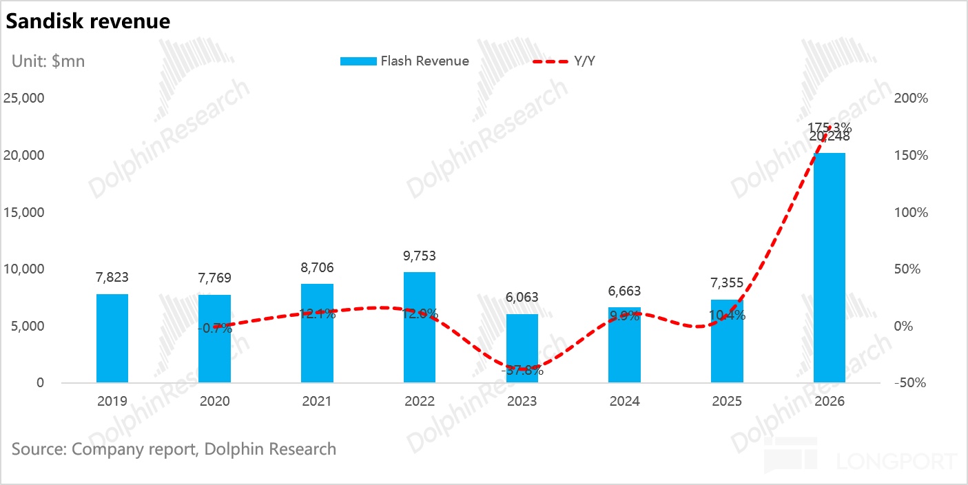
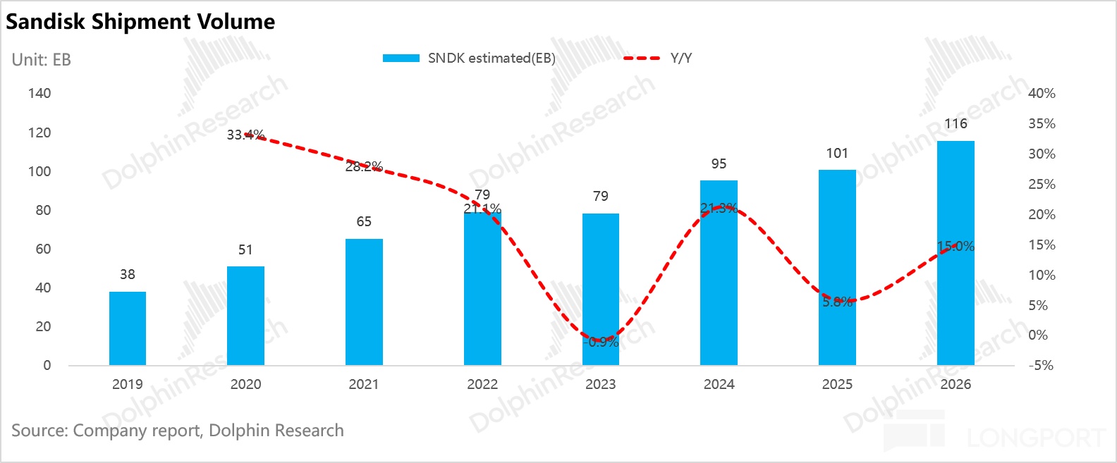
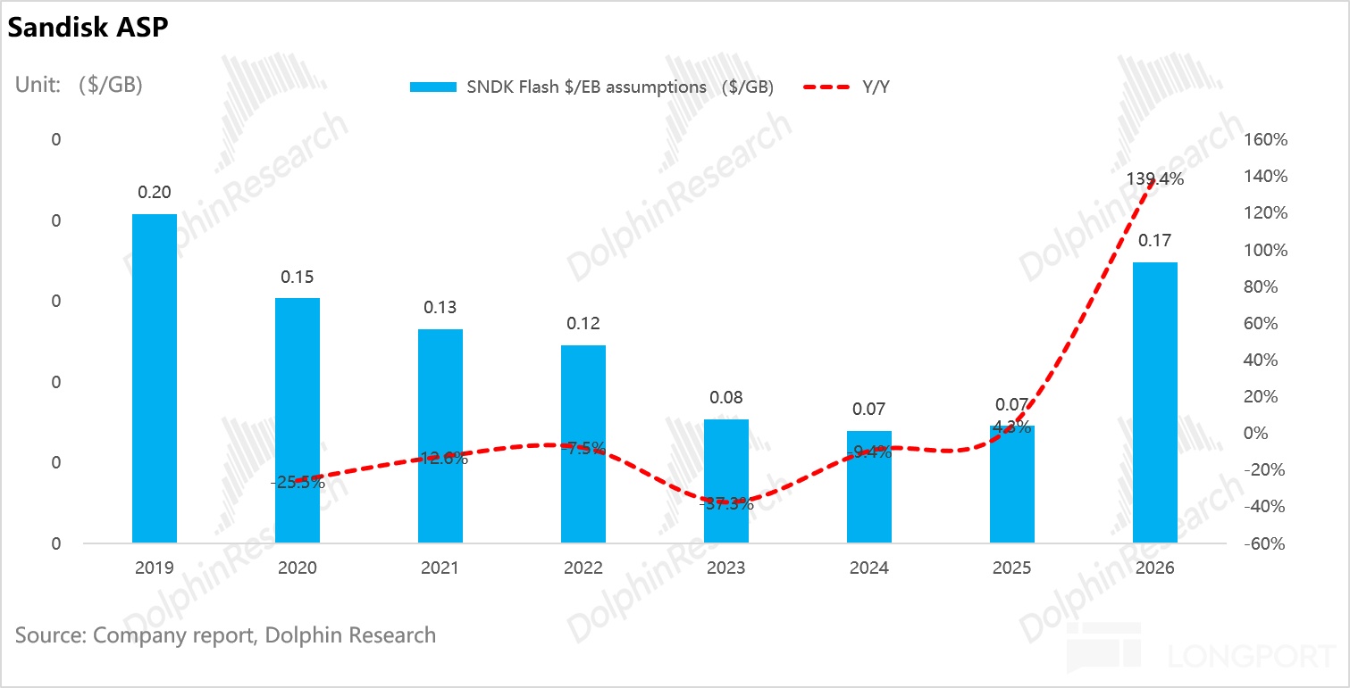
This reveals NAND’s harsh reality: there is no stable link between doing more volume and growing revenue. Cost downs from tech progress are largely handed to customers, leaving little value capture for manufacturers.
① In the down-cycle, revenue collapse is price-driven while volume still grows.
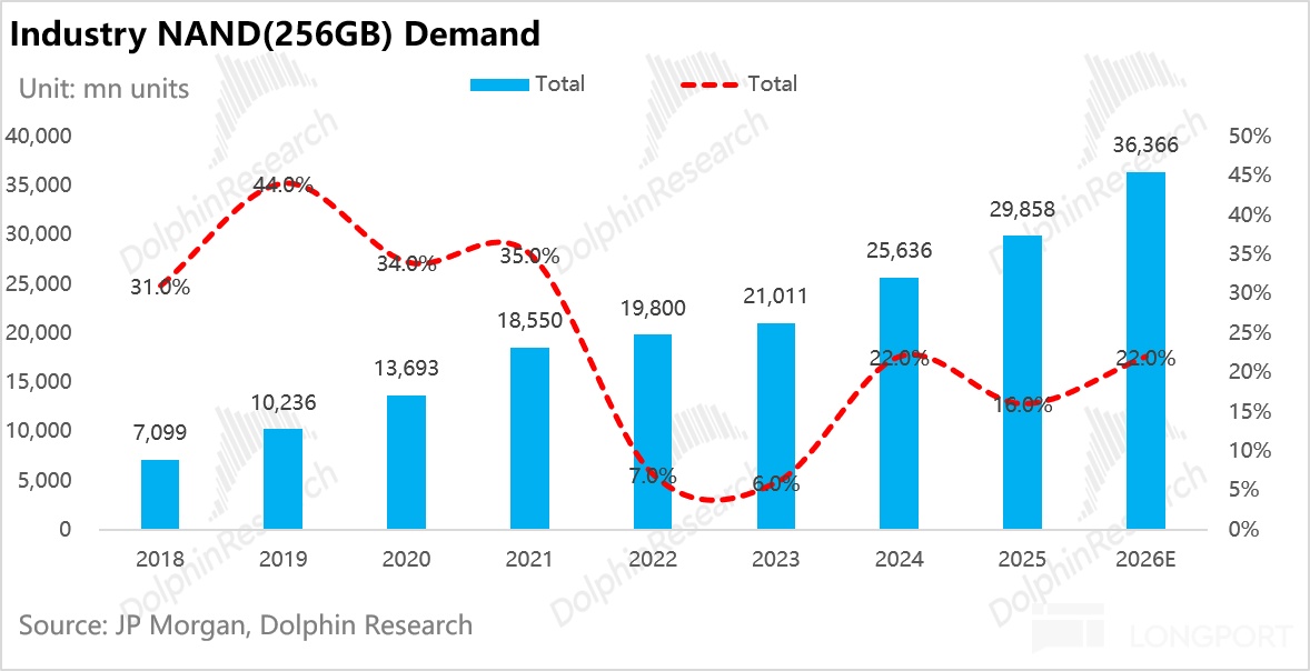
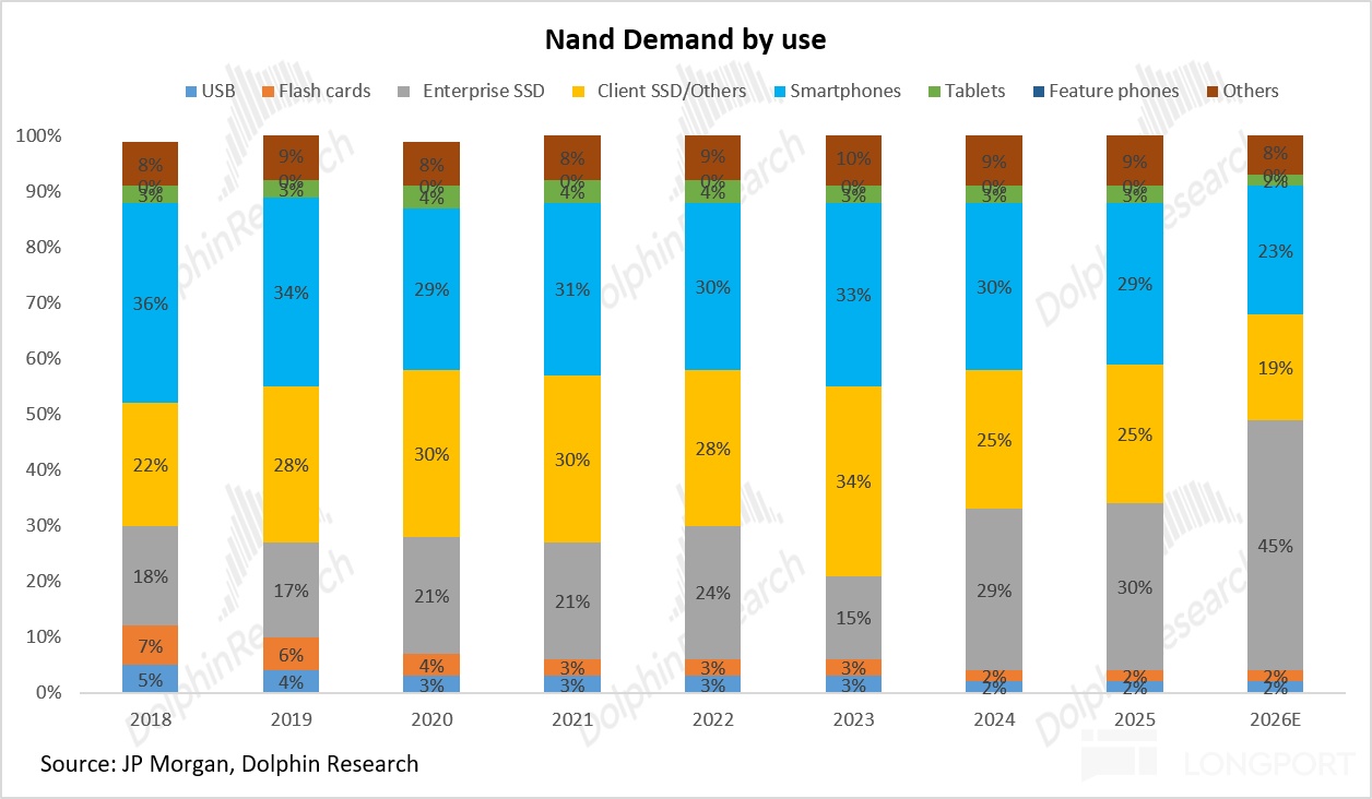
NAND end-demand grew 30%+ annually in 2018–2021 (34%–46%) on three forces. The uplift was broad-based.
a. Smartphones proliferated with capacity upgrades, as each flagship generation doubled storage. This drove mobile NAND bit demand to grow at a 34% CAGR in 2018–2021.
b. PCs shifted from HDD to SSD as client SSD penetration rose from ~50% to 90%+. From 2019–2021, client SSD bit demand grew 34%+ for three straight years.
c. Enterprise SSD expanded as cloud servers accelerated SSD deployment. The standard server cycle was strong.
But in 2022–2023, demand growth decelerated sharply to just 6%–8%.
a. Handsets contracted across the board. As the largest single end-market (~33% of bit demand in 2023), inflation and rate hikes hurt upgrades on top of pandemic pull-forward in 2021, driving mobile bit growth from 46% in 2021 to 2% in 2022.
b. PCs fell off a cliff. Pandemic WFH demand pulled forward the cycle, with global PC shipments −12% YoY in 2022 and another −10% in 2023.
c. Enterprise SSD cooled as standard servers digested the 2021 capex peak. Enterprise SSD bit demand slowed from +34% in 2021 to +20% in 2022 and turned −33% in 2023, while AI servers were not yet large enough to offset.
d. The inventory bullwhip magnified the contraction as all three end-markets de-stocked. OEM inventory rose from 6 to 16 weeks, and a self-reinforcing price-drop expectation pushed buyers to delay and shift to JIT orders, further pressuring price and amplifying order volatility vs. relatively modest end-demand growth.
For SanDisk, 2023 shipments were flat, while ASP/GB and revenue both fell 37.8% YoY. At the industry level, revenue was down ~37% with ASP down ~42%, implying price drove the full decline.
This differs from classic cyclical sectors like steel, chemicals, and shipping where down-cycles see demand shrink, volumes drop, and price stabilize via curtailments. In NAND’s worst year, producers cut, yet shipments did not contract, while price sank nearly 40%.
NAND traded like a commodity in this phase. Prices reflected market gamesmanship, tech and cost advantages did not translate into pricing power, and price declines fully swallowed the gains from volume.
2. Why does NAND supply fall into a 'can’t-cut' trap?
Producers did enact unprecedented deep cuts.
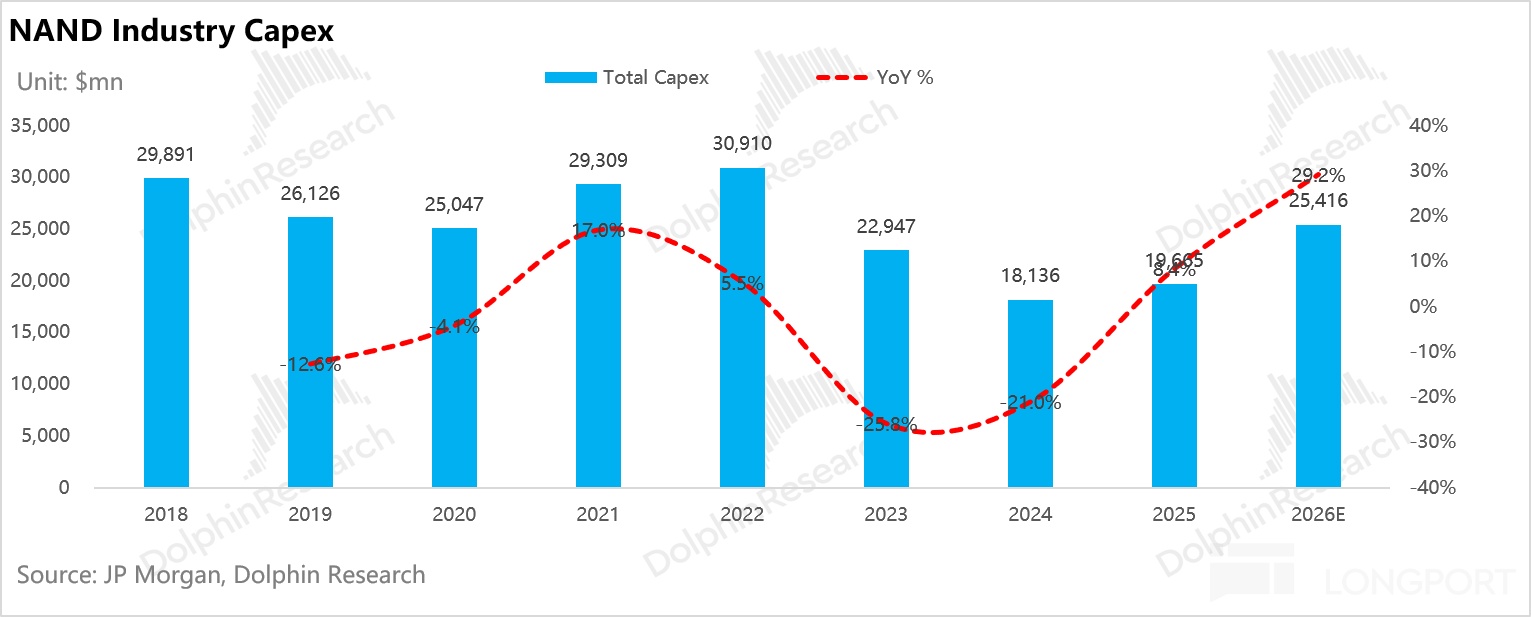
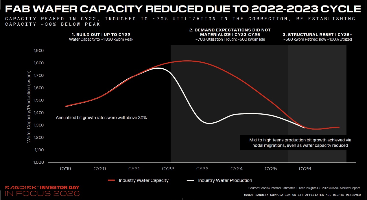
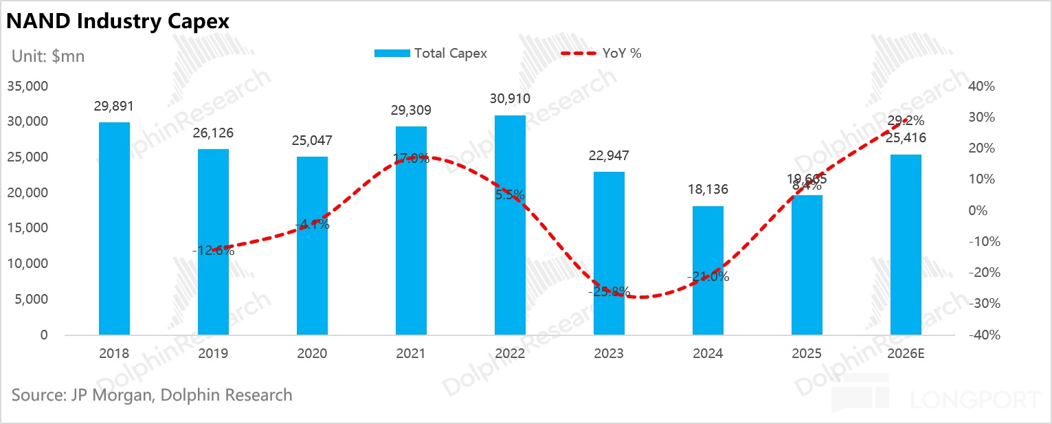
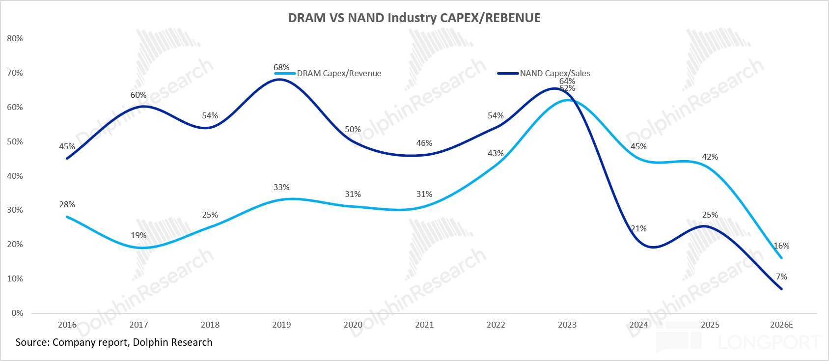
On capex, industry spend fell from a $30.9bn peak in 2022 for two straight years to a $18.1bn trough in 2024, down 41% cumulatively. This was a severe pullback.
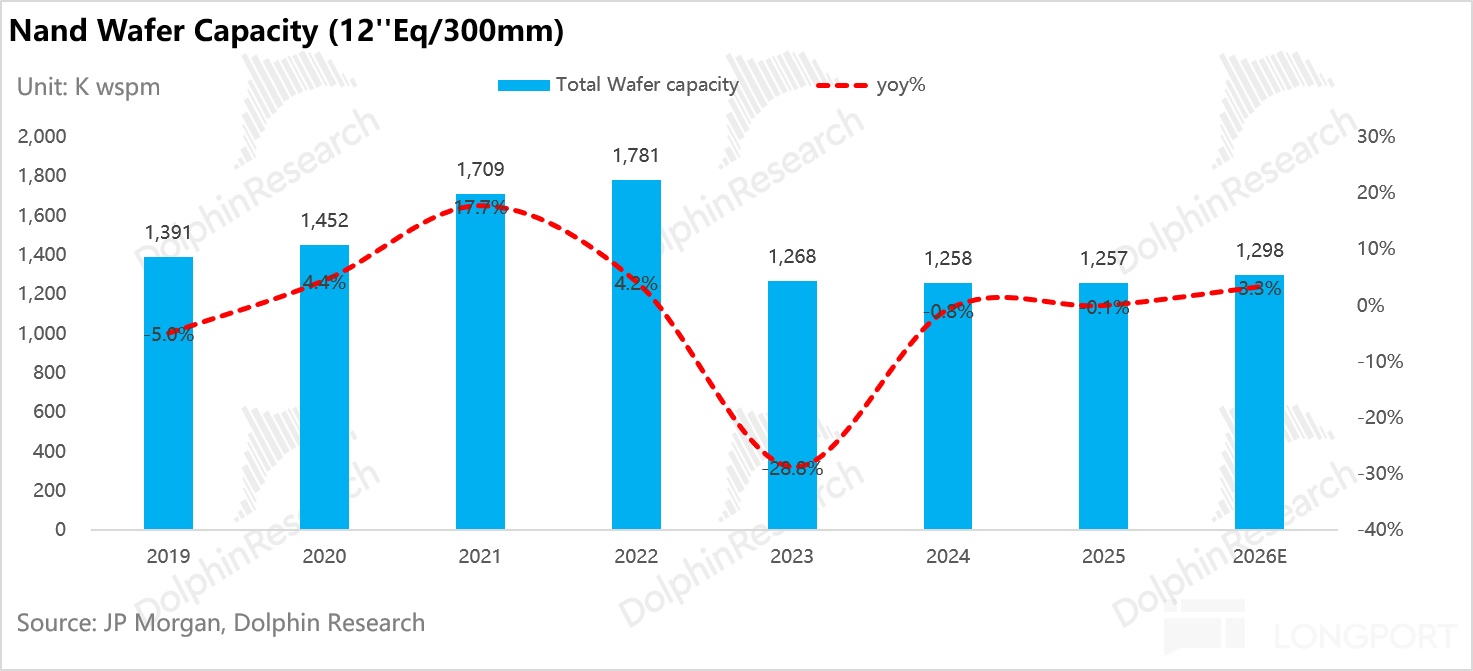
On wafer starts, monthly NAND wafers fell from a 1.78mn peak in 2022 to 1.27mn in 2023, down 28.8% YoY. SanDisk indicated utilization dropped to ~70% at one point, idling ~0.5mn wpm.
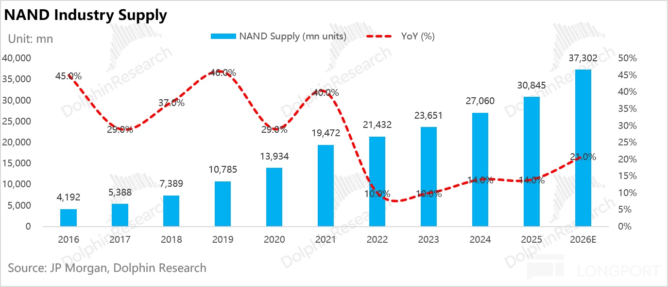
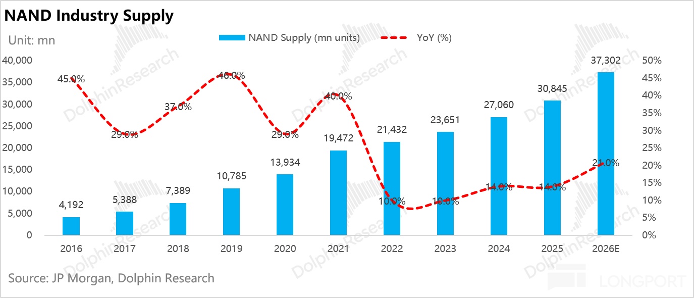
Yet supply did not contract: wafer starts shrank ~29% in 2023, but bit supply still grew ~10%. From 2016–2026, NAND bit supply never posted negative growth, even with industry revenue −37% and losses in 2023.
The divergence between fewer wafers and more bits came entirely from node migration and unit-wafer efficiency gains. The core issue is structural.
Root cause: NAND’s technology cadence inherently creates excess capacity via efficiency gains. Node moves are a built-in supply expander.
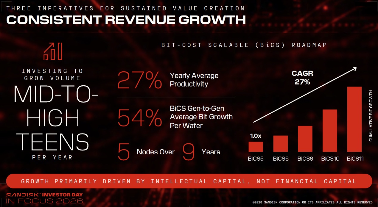
Per SanDisk, across five nodes from BiCS5 to BiCS11, bits/wafer rose ~54% per node on avg., or ~27% CAGR. That far exceeds the industry’s mid-to-high-teens long-term demand growth.
In other words, vendors can cut wafer starts but cannot cut the efficiency uplift embedded in each wafer. That portion of supply growth is automatic and independent of curtailment intent.
What drives bits/wafer to keep rising without higher capex or more starts?
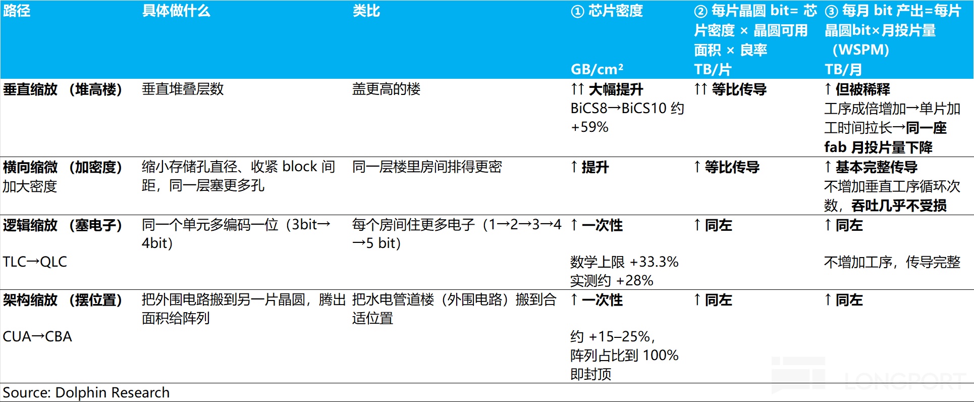
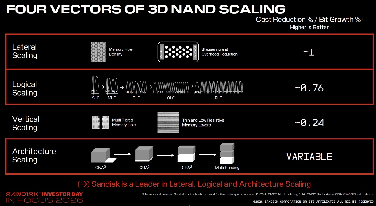
The metric decomposes into four levers. Each contributes differently over time.
Bits per wafer = hole density × layers × array area ratio × bits per cell.
'Logic scaling' and 'architecture scaling' are largely one-offs. The sustainable engines are more layers and denser lateral hole patterning, which NAND leaders grind out year after year.
① Logic scaling (TLC→QLC): a one-time step-up, not a repeatable driver.
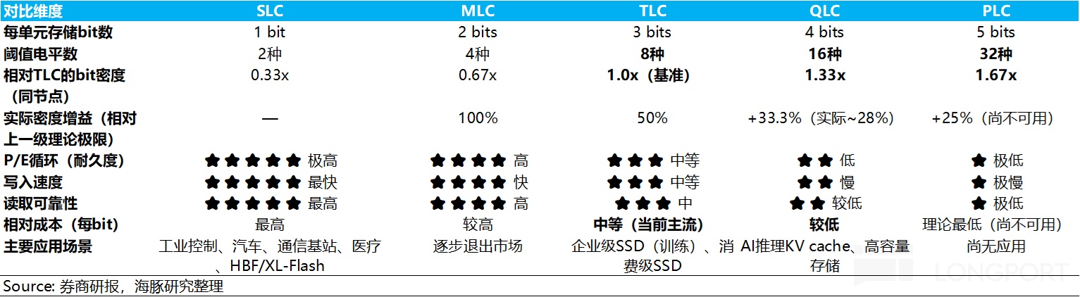
Cells encode information by threshold voltage, from SLC (1 bit) to MLC, TLC (3 bits), and QLC (4 bits). Capacity rises per cell without adding area.
The trade-offs are clear: QLC must resolve 16 levels vs. 8 for TLC, halving noise margin, slowing writes, and cutting endurance to roughly one-third of TLC. PLC would be worse, and SanDisk has not provided a timetable.
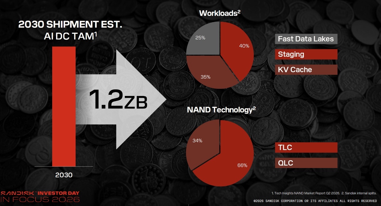
Importantly, the lever does not fully monetize structurally across use-cases. SanDisk positions TLC for performance-centric eSSD (KV cache data accessed less frequently) and QLC for capacity-centric eSSD (rarely accessed KV cache data).
SanDisk estimates AI datacenter flash TAM at 1.2 ZB by 2030 (similar to 2026 global shipments), with TLC at 66% and QLC at 34%. Even in an optimistic case, two-thirds of bits still sit with TLC in five years.
② Optimizing the placement of memory vs. logic: also a one-off, with value in performance more than density.
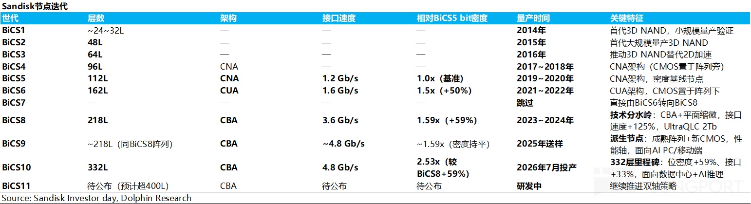
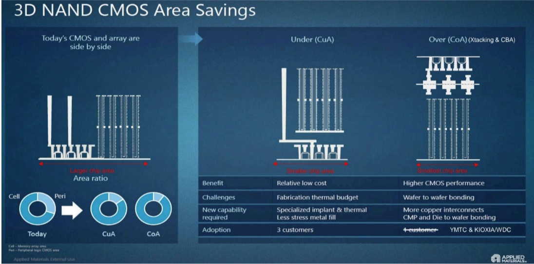
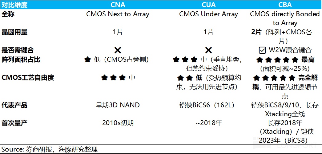
From a density view, CBA (CMOS bonded on Array) essentially reclaims dead area by separating the logic circuitry from the array and copper-to-copper bonding the wafers. The path has evolved from logic beside the array (CNA), to beneath (CUA), to fully split and then bonded (CBA).
But this reclaim has a hard cap: if logic was 20% of area and the array 80%, moving logic out takes the array to 100% and adds 25% density, with no further area to recover. YMTC achieved ~25% area reduction on a similar approach, or ~33% equivalent density.
For SanDisk, CBA’s real value is performance.
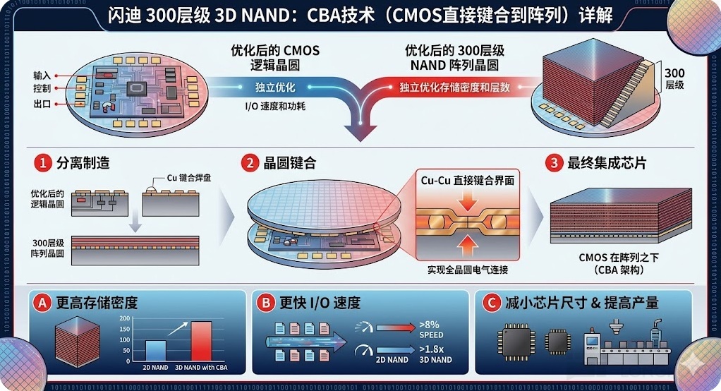
With copper bonding, logic and array process separately and then assemble, allowing logic CMOS to use a more advanced node at foundries for higher I/O and lower power. This yields speed and efficiency gains with minimal incremental capex.
Product-wise, vs. BiCS8 2Tb QLC, simply moving logic to a more advanced node in BiCS9 drives +150%/+75% write/read bandwidth and +85%/+40% write/read energy efficiency. The cost uplift is small.
Additionally, hybrid bonding and multi-wafer stacking underpin HBF. The first HBF arrays build on BiCS8, SanDisk’s first CBA node.
③ Vertical scaling: no single hard physical limit, but the economic limit is closing in fast.
3D stacking is the mainstream path to capacity, and vendors prioritize max layer count. There is no single physical cap, but costs and complexity surge under four constraints.
a. The capacity-dilution trap: more layers multiply etch/deposition steps, increasing cycle time per wafer and reducing wpm. From 176L to 300L+, per-die capacity might rise 50%–60%, but bits out do not increase that much due to elongated process flow.
b. The multi-deck penalty: due to high aspect ratio limits in channel etch, single-deck tops out around 120–150L, forcing extra decks above that with repeated full process loops.
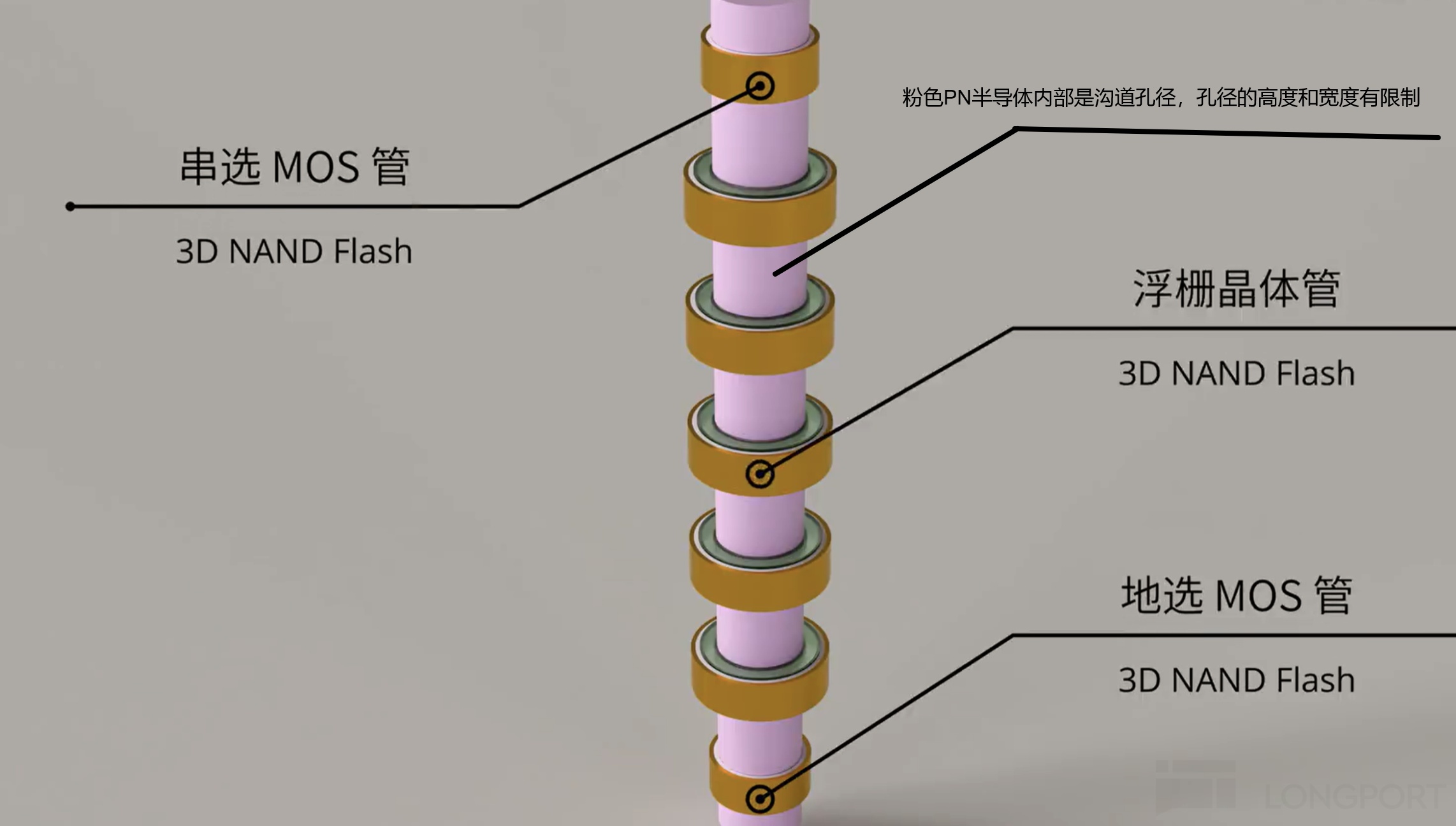
c. Forced material migration: around 300L with two decks, tungsten resistance and leakage become prohibitive, requiring a switch to molybdenum. Deposition and etch tool capex per 10k wpm nearly doubles.
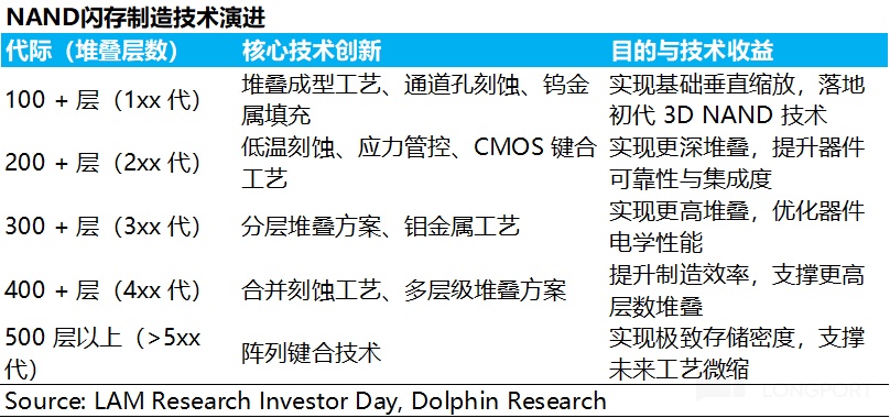
d. Array bonding and stress at 500L+: oxides deform beyond this range, and further scaling needs wafer-to-wafer bonding akin to HBM, with complexity spiking.
Translation: beyond 500L, stacking needs bonding capabilities as a prerequisite. Kioxia/SanDisk led mass production of CBA starting with BiCS8 and have accumulated know-how here.
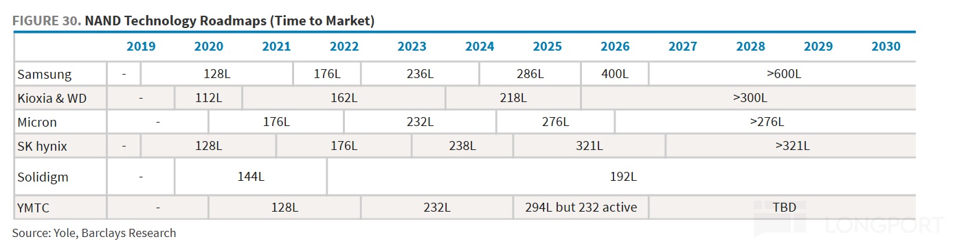
④ Lateral scaling: shrink holes and tighten block pitch, the most differentiated engine.
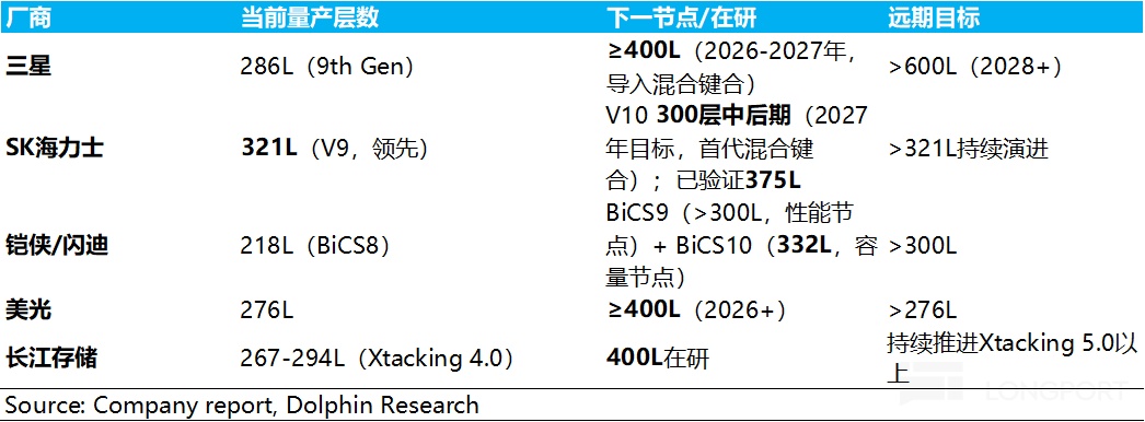
Layer-count race (taller stacks) is Samsung and SK hynix’s focus, leveraging DRAM know-how. Kioxia/SanDisk emphasize planar density and optimized functional layouts.
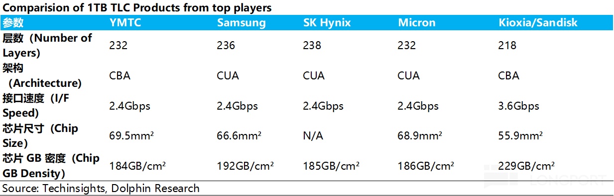
The lateral game hinges on etch innovation to pack more pillars in-plane. As a result, Kioxia/SanDisk achieved the highest 229 GB/cm² density with only 218 layers, 29% more density per layer than the next best, and the smallest die at 55.9 mm², ~16% smaller than Samsung, yielding ~19% more dies per wafer.
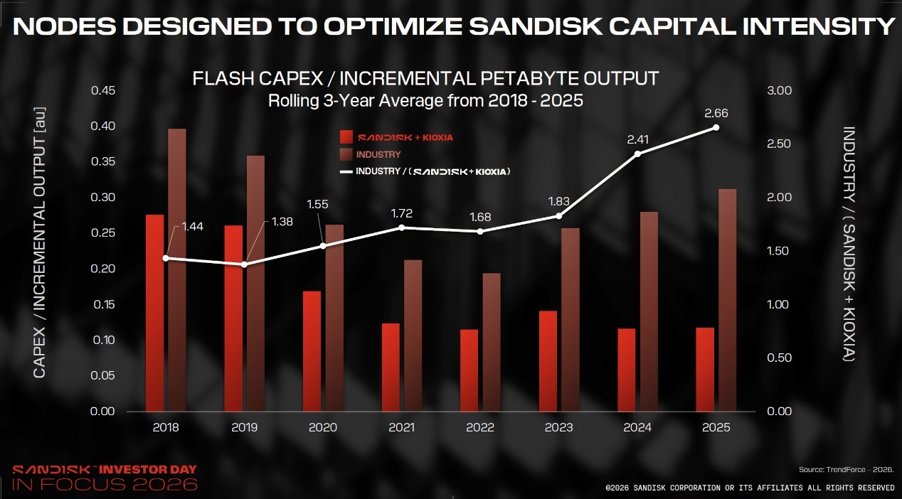
The strategic gap is capital intensity: Samsung/SK hynix spend more steps and tools to lead on layers, while Kioxia/SanDisk use fewer layers to hit higher density with fewer steps and tools. This shows up in capex efficiency.
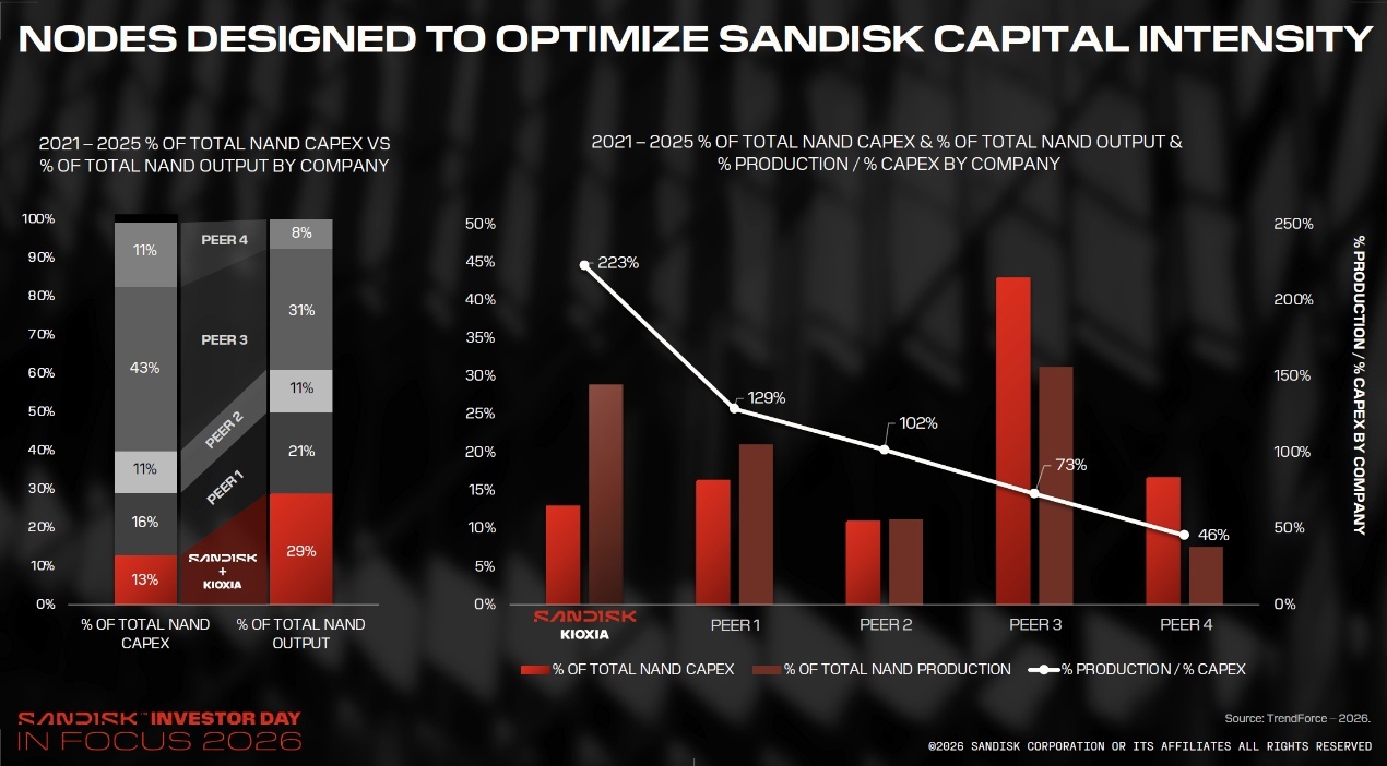
In 2025, industry capex per incremental PB is 2.66x higher than the Kioxia/SanDisk JV. From 2021–2025, they produced 29% of bits with just 13% of industry capex.
3. What are the fundamental supply-side differences between NAND and DRAM?
NAND and DRAM expand supply under two very different physical regimes, which drive divergent capital intensity and cyclicality. The difference is physical, not just strategic.
Supply expands via two routes: node migration (more bits per die, a stock upgrade) and higher wafer starts (new cleanrooms and tools, an incremental build). The former consumes far less capital.
Migration efficacy depends on how fast density can still rise. There are two paths.
a. Vertical: stack more layers with active cells on each layer. b. Lateral: shrink cell pitch to fit more per layer.
NAND can do both, stacking for multiplicative density and shrinking laterally. DRAM on a single wafer base is essentially lateral-only, as each cell has a vertical deep trench capacitor that cannot be stacked cost-effectively like NAND’s one-shot multi-layer etch.
This caps migration output: DRAM node density gains are ~10% per gen (1b→1c now below 10%), while NAND still sees 50%–60% per gen. Thus DRAM bits/wafer rise only ~5%–10% p.a. from migration, far short of demand, forcing new cleanrooms, whereas NAND migration alone can meet or exceed demand growth.
Why can’t DRAM stack vertically like NAND?
3.1. NAND 3D stacking: scale via batch formation and serial sharing.
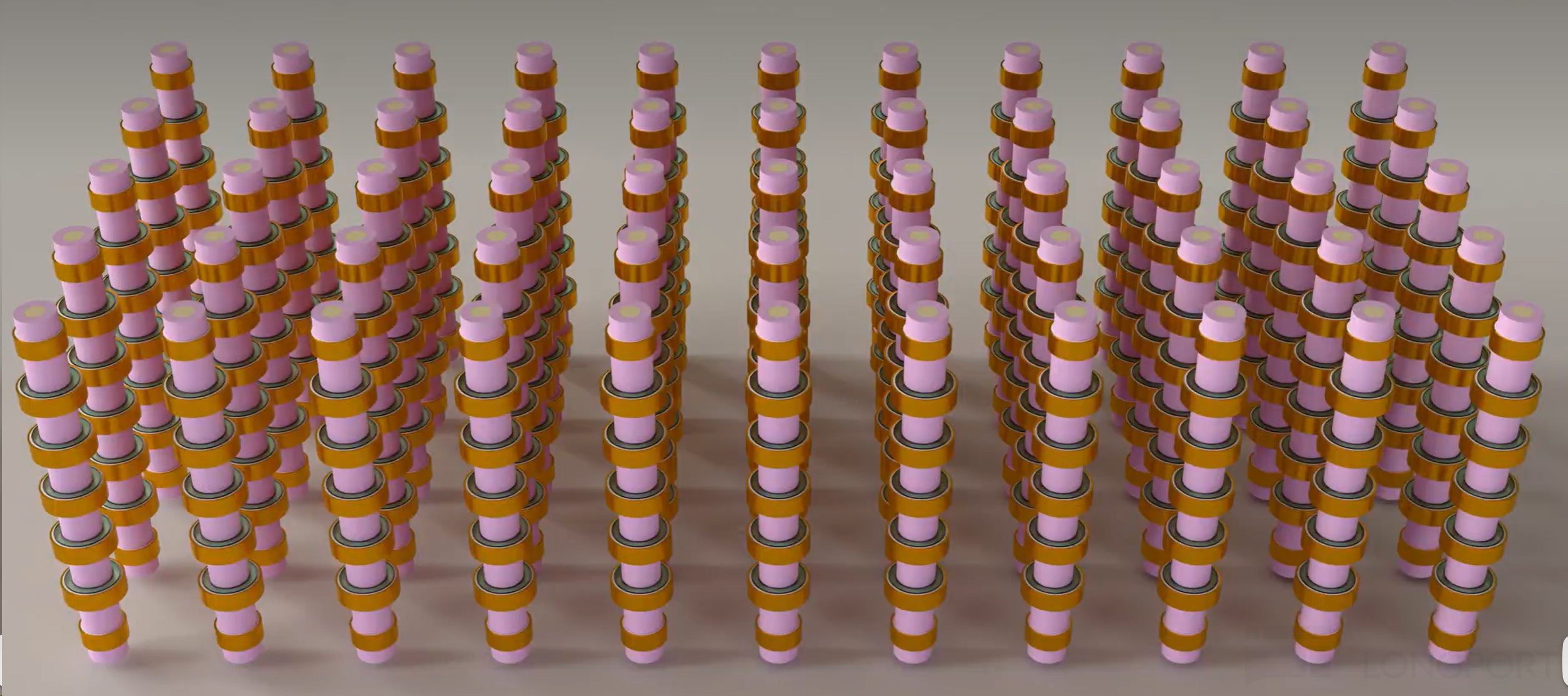
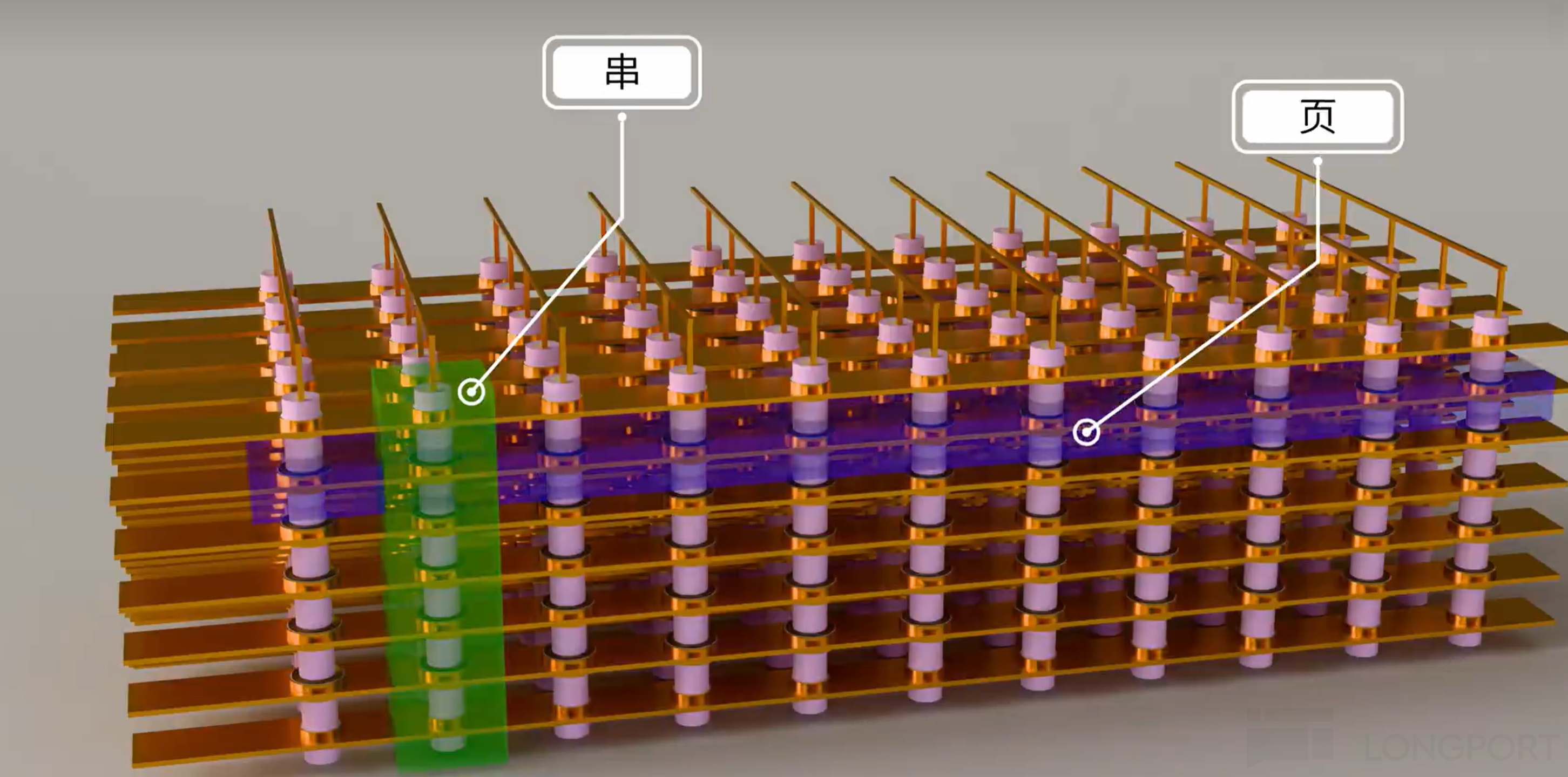
a. Serial sharing: NAND cells are switchable transistors, connected in series along one vertical channel to share a bitline. To read a target layer, apply pass voltage to other layers to act as wires so current reaches the target.
b. Batch formation: 3D NAND is built like a cast, alternately depositing hundreds of oxide/nitride layers, then punching through them once with HAR etch and filling channels so hundreds of cells form simultaneously.
NAND cells are defined by intersections, not individually placed devices. Each deposited layer becomes a wordline like painting a wall, while the costly patterning is the single channel etch that creates hundreds of cells per shot.
Cost hinges on asymmetric process composition: more layers add mostly deposition (repeatable, cheaper), while the high-cost litho/etch count that defines channels does not scale with layer count. This is why stacking is capital efficient.
DRAM: constrained to 2D, stuck with heavy capex expansion.
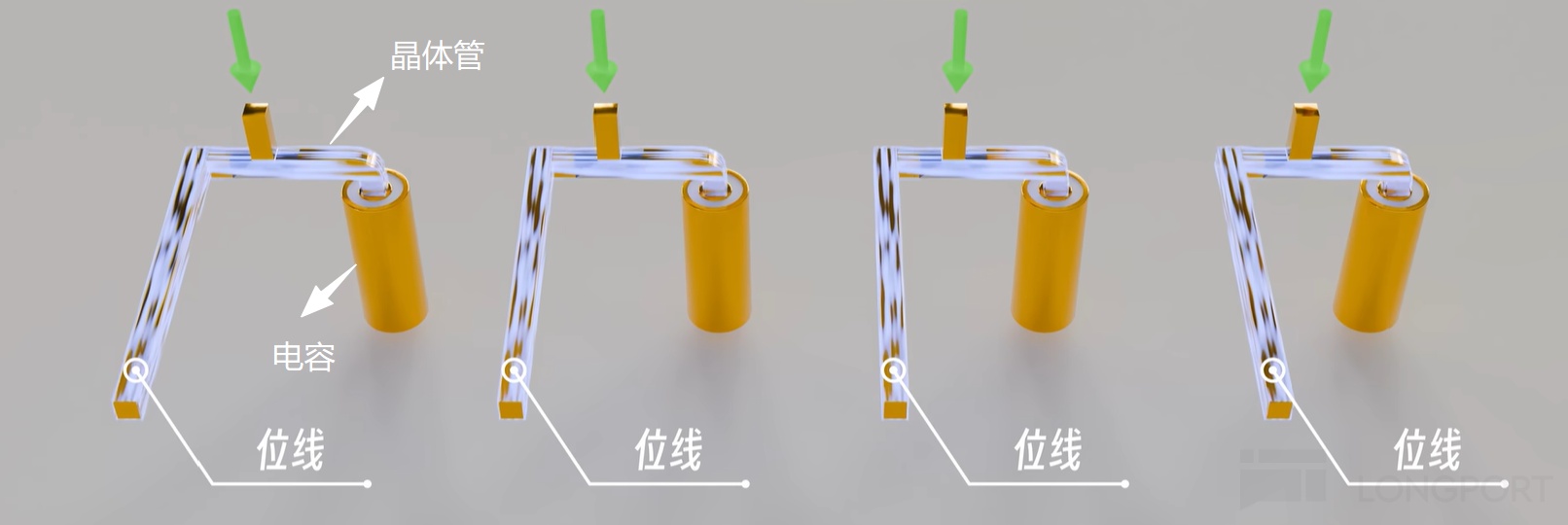
a. Physical root cause: capacitors don’t conduct DC, so cells can’t be chained.
Each DRAM cell is 1T1C, and the capacitor blocks DC, preventing NAND-like serial chains. You cannot pass current through even the first capacitor, so there is no serial sharing.
NAND can tolerate opening many upstream cells because it moves KB–MB pages and amortizes overhead. DRAM must fetch arbitrary addresses in tens of ns as CPU memory, leaving no room to amortize.
Therefore DRAM cannot share bitlines vertically, as each added layer would need its own routed line from the bottom. This is physically prohibitive.

b. HBM further widens the capacity gap.
As lateral scaling slows for per-die capacity, HBM emerged to solve bandwidth and capacity in a tight package footprint. Effective capacity equals per-die capacity times the number of die layers.
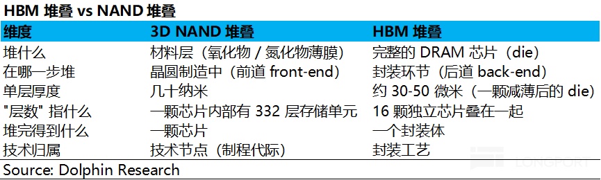
But NAND and HBM stacking are fundamentally different.
NAND is like building 300–400 floors on one shared foundation in one process, getting cheaper with height and not consuming extra wafer area. HBM is like stacking separate houses each with its own foundation, drilling TSVs and aligning per die, getting more expensive with height and consuming far more wafer output.
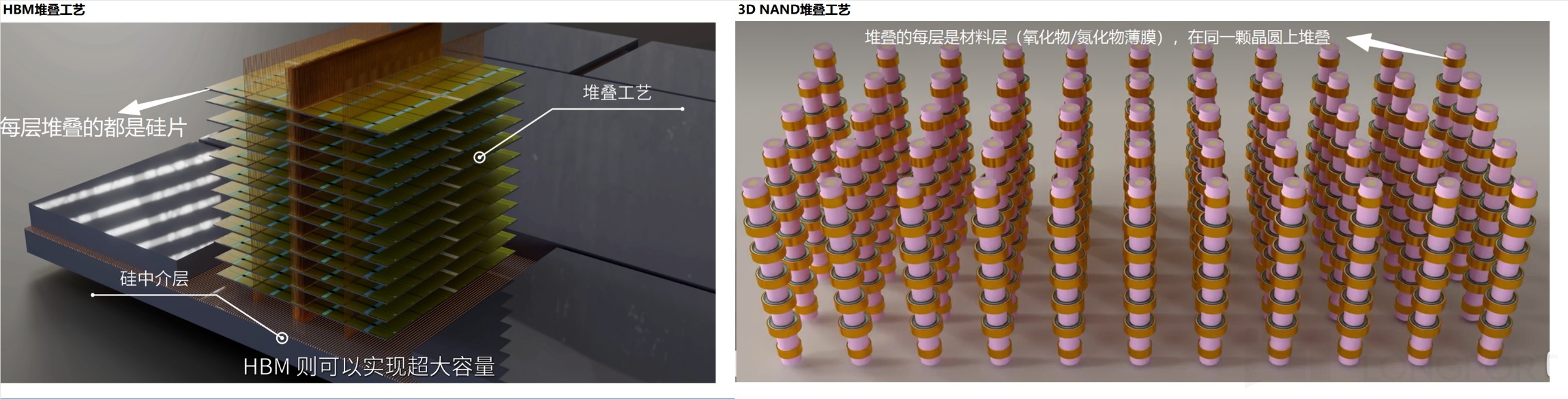
With DRAM migration adding only 5%–10% bits annually, HBM’s rise blows out the shortfall with three multipliers on wafer consumption.
a. Larger die as TSVs and complex I/O reserve keep-out zones, inflating die size vs. DDR for the same capacity. b. Multi-die stacks (8–16 high) multiply die needed per HBM unit.
c. Composite yield is structurally lower after stacking due to dicing/bonding loss and compounding yields. Together, producing the same bits on HBM consumes ~2–3x the wafer capacity vs. standard DDR.
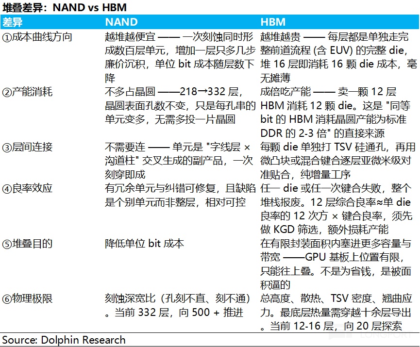
The gap must be closed by building new cleanrooms, explaining why 2024–2026 DRAM and NAND capex diverge sharply.
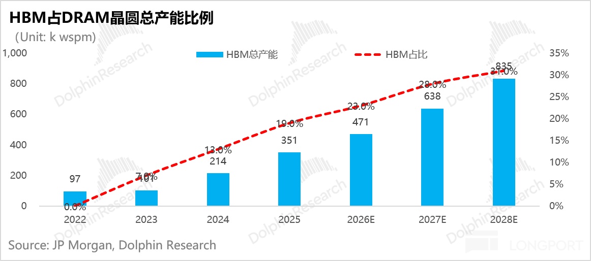
HBM crowd-out is the core of this capex wave. HBM’s share of global DRAM wafers rises from 7% in 2023 to 23% in 2026, with absolute capacity from 100k wpm to 470k wpm, more than tripling in three years.
HBM’s capacity efficiency is far below standard DRAM: die area is roughly 3x, so a wafer yields 1,500–1,800 DDR dies but only 500–600 HBM dies. Add 8–16 die per stack and yield compounding, and effective bits per wafer drop materially.
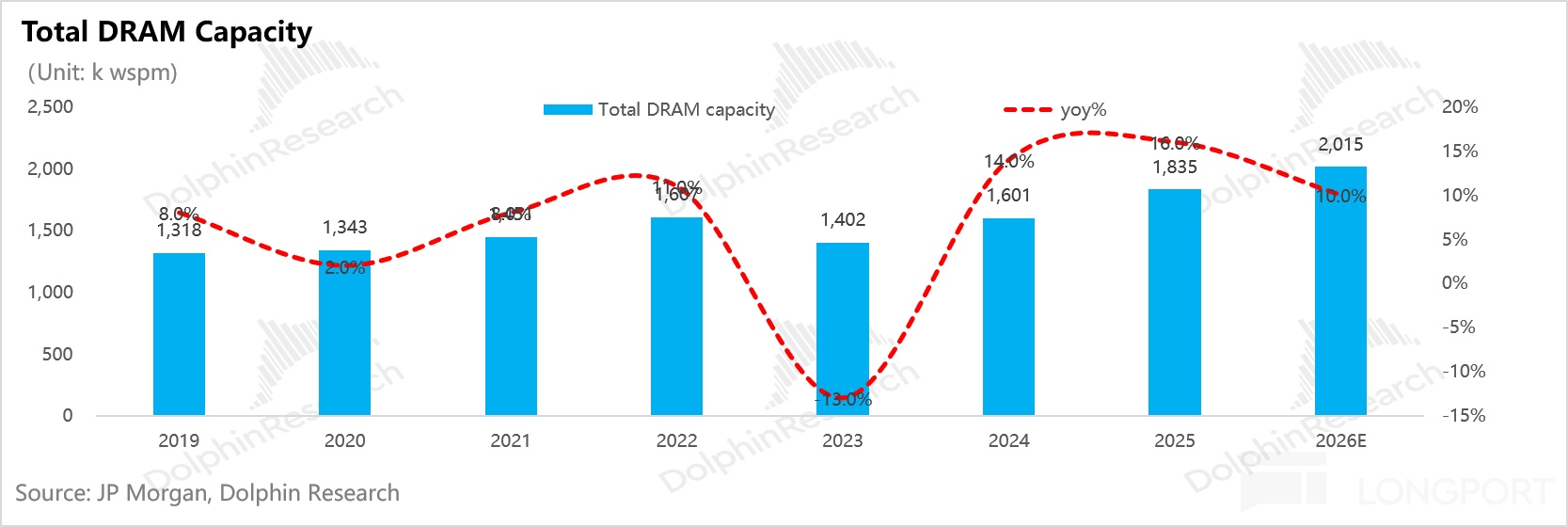
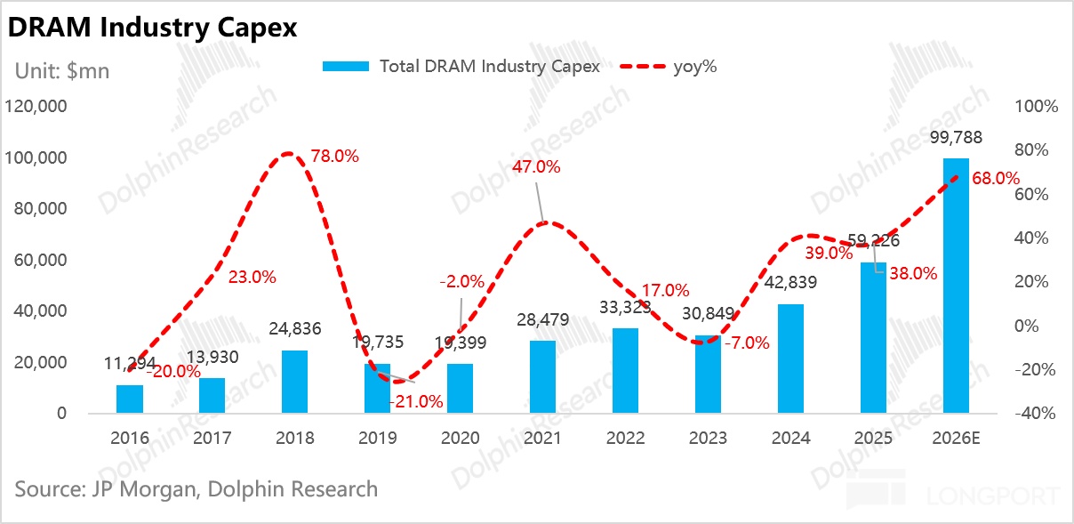
Thus DRAM capex keeps climbing: from $30.8bn in 2023 to $99.8bn in 2026E (+68% YoY at peak). Global DRAM capacity fell −13% in 2023 then resumed expansion to 2.02mn wpm in 2026E vs. 1.40mn in 2023, ~25% above the 2022 peak.
Meanwhile, NAND capex is rebounding off a $19.7bn trough in 2024 (+21% in 2025, +29% in 2026), but the 2026 level of $25.4bn remains ~18% below the 2022 peak. The spend profiles have flipped.
In 2026, DRAM capex is ~$99.8bn (top-3 at ~$87.7bn), while NAND is ~$25.4bn. DRAM is nearly 4x NAND.
On capital intensity, DRAM capex/revenue is ~16% in 2026 vs. ~7% for NAND, consistent with SanDisk’s long-term guide of mid-to-low single digits. The structural gap persists.
This mirrors two supply logics in one cycle: DRAM needs new fabs for HBM, while NAND can meet growth through node migrations.
4. Why do DRAM and NAND diverge so much despite shared origins?
Both are highly cyclical, but physical differences drive very different business models.
a. Asymmetry in cycle dynamics: NAND’s down-cycles are harsher, DRAM’s adjustments are more controlled.
NAND’s down-cycles are brutal because migration auto-expands supply as layer counts rise, even with capex cuts. The 3D transition also produced a one-time step-up that overshot demand for a period.
DRAM’s down-cycles are milder as migration gains keep slowing and lag demand, making expansion dependent on new cleanrooms. Cutting capex tightens supply quickly in the physical sense, giving DRAM more downside resilience but slower upside capacity adds.
b. Pricing power foundations differ: DRAM relies on physical moats, NAND on industry discipline.
DRAM, especially HBM, is tight due to real physical capacity constraints and extreme manufacturing complexity. TSVs and advanced bonding enforce differentiation, pushing the Big 3 to tilt capacity toward HBM and tightening standard DDR further.
By contrast, NAND’s current tightness leans on oligopoly discipline. SanDisk is actively capping industry bit growth at ~15% instead of the historical 30%+ pace.
This implies significant latent technical supply remains parked and can be unleashed without massive new capex. It creates big upside elasticity and uncertainty in up-cycles.
Once discipline loosens or China players accelerate builds, the over-supply sword can drop quickly. The risk is ever-present.
c. Cash flow and returns diverge: NAND morphs into a cash cow.
DRAM must recycle operating cash into heavy capex continuously, with a single leading-edge fab already costing $20bn+. NAND capex is mostly node upgrades on existing lines rather than greenfield expansion.
For SanDisk, long-term guides are attractive: capex at mid-to-low single digits of revenue, adj. FCF margin around 50%, and 100% of excess cash to buybacks. It is a structurally cash-generative model.
Even though SK hynix announced a KRW 40tn buyback in Aug-2026, signaling DRAM’s pivot to shareholder returns, its structurally higher capital intensity means cash generation should still trail the lighter-asset NAND model over a super-cycle.
Bottom line, if NAND supply can 'auto' grow bits while the Big 3 prioritize DRAM/HBM, watch two things. First, whether other vendors break discipline and expand NAND. Second, how durable AI-driven NAND demand proves to be.
So, under the AI wave, are others truly holding the line on NAND capex? How is end-demand reshaping mix structurally, how long can this pricing super-cycle run, and at current valuation, does post-rebirth SanDisk still have upside?
Dolphin Research will tackle these in the next note. Stay tuned.
<End>
Risk disclosure and statement: Dolphin Research disclaimer and general disclosure


The copyright of this article belongs to the original author/organization.
The views expressed herein are solely those of the author and do not reflect the stance of the platform. The content is intended for investment reference purposes only and shall not be considered as investment advice. Please contact us if you have any questions or suggestions regarding the content services provided by the platform.